
onsemi MC74ACT00D Quad 2-Input NAND Gate: Datasheet, Pinout, and Application Circuits
The MC74ACT00D from onsemi is a member of the advanced high-speed CMOS (ACT) logic family, integrating four independent 2-input NAND gates in a single package. Renowned for its high noise immunity and low power consumption characteristic of CMOS technology, it also provides the high speed and output drive of TTL, making it a versatile choice for a wide array of digital logic applications.
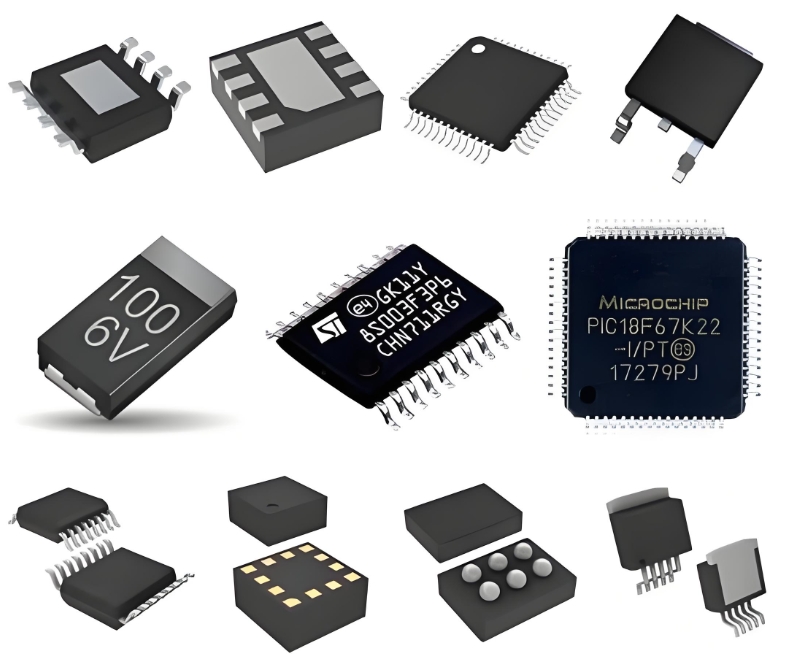
This device is supplied in a common 14-pin SOIC package, making it suitable for space-constrained PCB designs. Its robust performance and reliability have cemented its status as a fundamental component in modern electronic circuit design.
Datasheet Overview and Key Specifications
A thorough review of the MC74ACT00D datasheet is essential for proper implementation. Key absolute maximum ratings and electrical characteristics include:
Supply Voltage (VCC): 7V
Input Voltage (VI): 7V
Operating Temperature Range: -55°C to +125°C
High-Level Output Current (IOH): -24mA
Low-Level Output Current (IOL): 24mA
The ACT family's defining feature is its TTL-compatible input thresholds, which allow it to be driven directly by TTL outputs without requiring extra components. Furthermore, it boasts a typical propagation delay (tPD) of just 5 ns at 5V, enabling its use in high-frequency circuits. Its fanout is substantial, capable of driving up to 50 ACT inputs.
Pinout Configuration
The pinout of the MC74ACT00D follows a standard layout for a 14-pin Quad 2-Input NAND Gate IC:
Pin 1: Input A (Gate 1)
Pin 2: Input B (Gate 1)
Pin 3: Output Y (Gate 1)
Pin 4: Input A (Gate 2)
Pin 5: Input B (Gate 2)
Pin 6: Output Y (Gate 2)
Pin 7: Ground (GND)
Pin 8: Output Y (Gate 3)
Pin 9: Input B (Gate 3)
Pin 10: Input A (Gate 3)
Pin 11: Output Y (Gate 4)
Pin 12: Input B (Gate 4)
Pin 13: Input A (Gate 4)
Pin 14: Supply Voltage (VCC)
Application Circuits
The NAND gate is a universal gate, meaning any other logic function can be constructed from it. The MC74ACT00D is incredibly versatile.
1. Basic Logic Function: Its primary use is to perform the logical NAND operation (Y = NOT (A AND B)), serving as a building block in complex circuits like adders, multiplexers, and memory units.
2. Oscillator / Clock Pulse Generator: By connecting the outputs of two gates back to the inputs with resistors and a capacitor, a simple astable multivibrator (oscillator) can be created. The oscillation frequency is determined by the RC time constant.
3. Set-Reset (SR) Latch: A basic bistable multivibrator (latch) can be constructed using two cross-coupled NAND gates. This circuit can store a single bit of data, forming the foundation of flip-flops and memory cells.
4. Debouncing Circuit: Mechanical switches produce bouncing signals that can be misinterpreted as multiple presses by digital circuits. A NAND gate-based SR latch is an effective and simple solution to debounce these signals, ensuring a single, clean logic transition.
ICGOODFIND: The onsemi MC74ACT00D stands as a quintessential logic IC, offering a perfect blend of high-speed performance, significant output drive capability, and CMOS low power consumption. Its TTL-compatible inputs ensure easy integration into both new and legacy systems. Whether used for basic logic, signal conditioning, or clock generation, this device provides a reliable and efficient solution for countless digital design challenges.
Keywords
1. MC74ACT00D
2. Quad 2-Input NAND Gate
3. TTL-Compatible
4. High-Speed CMOS
5. Application Circuits